- Dataflow
- Behavioral
- Structural
In this tutorial I will describe the same circuit using all 3 types of description so you can see the difference between them.
The designed circuit
A very simple but useful circuit is the parity detector. To determine the parity of a binery number we need to count the '1' bits. If that number is even than it is of even parity. If it's odd than the number is of odd parity. My tutorials will describe a circuit that outputs the even parity.
Parity detector with 3 inputs and 1 output truth table:
A B C O
0 0 0 1
0 0 1 0
0 1 0 0
0 1 1 1
1 0 0 0
1 0 1 1
1 1 0 1
1 1 1 0
So when the number of '1's is enev the output is '1' and vice versa.
As you can see the truth table is rather large so it needs to be minimized. Since logic function minimization is out of the scope of this tutorial I will not be presenting it but there are lots of articles on the internet about the ways to do it.
The circuit we will describe looks like this:

There are other ways to design the logic diagram but using XOR gates is the most simple circuit for detecting parity.
Regardless of the way we will describe the circuit, the entity will remain the same:

Dataflow description
In dataflow we describe circuits using only concurrent statements, mainly signal assignments.
A signal can be seen as a wire between 2 circuits. For example in the upper diagram abSIG is a signal that connects the first XOR output with the second XOR input.A, B, C and O are signals also but they connect the entity with the FPGA pins.
For this circuit we can use a description with signals or we can write the whole logic function in one statement. I will demonstrate both approaches.
Without signals:
You just have to write in the architecture
o <= not(a xor b xor c);

With signals:
For this method we need to declare 2 signals like those in the diagram. They will be of type STD_LOGIC.
The code looks like this:

Remember that the order of the statements is not set in stone because they take effect at the same time.
Behavioral description
This type of description uses sequential code that needs to be written inside a structure named process. The process is located in the architecture body and there can be more of them in the same architecture. Processes execute concurrently with each other but in each process the code is sequential.
Declaration of a process:
name: process(sensitivity list)
The name is not necessary but when you have lots of processes it helps to easily find the one you want. The reserved word process is mandatory.
The sensitivity list is a list of signals that control the entrance in the process. That means that when a signal in the list changes value the process will execute it's code so you need to be careful to put all the necesary signals in that list.
After this line we can declare variables to use for the process. Variables, if you recall are local to each process they are declared in and help you build complex algorithms and circuits.
The code of the process comes next. It is enclosed in begin-end statements.
For this example we will not be using variables. The code looks like:

If you look at the sensitivity list you can see that every time one of the inputs changes it's value the process will run o will take a new value.
If we use signals the code will look exactly like for dataflow but it is important to keep it exactly the same because in processes code is sequential. This means that if you decide to put the o assignment first your code will be incorrect.
Structural description
This type of description is mostly used for more complex projects because you can segment your code in smaller circuits and connect them together using signals, hence the word "structural".
For our circuit we will need to make a description for the xor gate and one for the not gate. After that we will make another description of the main circuit in witch the others are connected.
Because this method is more complicated I will be walking you through the steps.
First create a new project with and give it a name:

After that set your device parameters, click next and click finish.
We are ready to start the coding. Create an entity and name it xorGate. It will have 2 inputs (i0 and i1) and 1 output (o). After it is created write in the architecture body: o <= i0 xor i1;

Now create another entity named inverter. It will have 1 input (i) and 1 output (o).

These are the 2 circuits needed for the main architecture.
Before we continue let's see a block diagram of our project:

As you can see the main description will have 3 inputs (A, B and C) and 1 output (O).
Because The main circuit and the 2 gates are in different files we need a way to link them. This is done of course in the main file using components. They are declared before the architecture begins (with the signals). There will be a component for each type of circuit (in our case one for andGate and one for inverter) and the structure of the component is exactly like that of the entity with 2 differences:
- instead of the entity keyword at the beginning we will use component
- instead of the name of the entity at the end statement we will use component as well
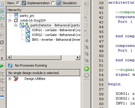
Let's create a new entity called parityDetector with the I/O specified and declare our 2 components:

After the components we need to declare our signals. These are used to link the components together.

Now it's time to link the components. Because there are 3 circuits in the block diagram we will be instantiating 3 components (2 xor gates and 1 inverter).
Each instantiation has 3 parts:
- A label that has to be unique for each component instantiation. It is placed first and it should have a suggestive name for that circuit
- The name of the component instantiated (the same name of the entity for the specific circuit)
- The reserved words "port map" followed by a list of signals in parentheses. The signals are the ones specified in the main entity (either the I/O of that entity or declared signals) and need to be placed in the order that the component has it's I/O placed. For example the inverter has it's I/O signals in the order: i,o so the instantiation for it would be:
INV: inverter port map(parity, O);
From that piece of code we conclude that the signal parity witch is also linked to the output of an xorGate is linked to the i pin of the inverter and the main output of our circuit: O is linked to the output pin of the inverter (o).
The code looks like this:

So the XORG1 circuit will compute an xor operation on A and B and communicate the result to XORG2 through the abSIG signal. XOR2 calculates abSIG xor C and gives the result to the inverter using the parity signal. The inverter performs the not operation and sends the result to the main output of the circuit. The order is not important because they are concurrent statements.
So the structural design is similar to a schematic design because we connect circuits with wires (signals). It is best used in more complex projects.
After you do the last bit of code save the project and the parityDetector entity should become the top level module:
Next put in the user constraints, implement and see the results.
For all the examples in this tutorial the inputs should be 3 slide switches and the output a LED.
No comments:
Post a Comment