Translate

Thursday, December 27, 2012

VHDL project using schematic view


       As projects get more and more complex it is more and more harder to build projects using structural description because mistakes can happen when connecting signal together. That's why we will see how to aggregate different circuits in one using schematic view in Xilnx ISE Webpack. The version that I am using is 13.4 so some thing might be different if you are using another version.
       In his tutorial we will build the same project that we did in my last post: Blinking a LED at different intervals but first let's see the basics of using the schematic mode.
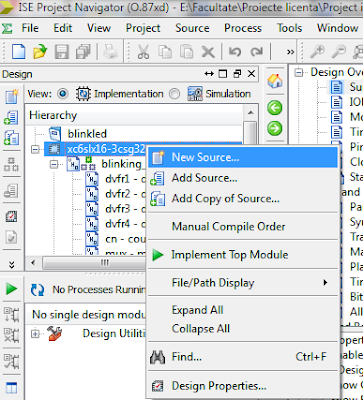
       To create a schematic mode cicuit right click the project and select New source:

       Now select Schematic and give the entity a name:
       After this click Next and then Finish and the entity is created. 
       Now the first ting you need to know is how to navigate through the project. In the left side of the window in the middle of the project screen is an Options menu open. To get to the list of circuits that you can put on the project just click the Symbols tab:

       The circuits from you current project can be found in Categories at your local path which for me is the one with "E:\Facultate.....". To get to the entity list click on Design from the same tabs list and you will get the familiar menu. Next thing we should cover is the instruments panel that is located next to the menus that we discussed about just now. 

       The first button from this panel is the Select button. You press it when you just want to click on a circuit in order to view it's properties for example. This button changes the mode you are in: for example if you are in line drawing mode you push this one to get out of it so you can view or edit other things.
       The second tool is the zoom tool. You press it and then drag around the area that you wish to zoom in. Zoom can also be achieved by using the buttons from the other instruments bar above the project window.
       The next button is used for connecting circuits. Just press it and then click on an input or output of a circuit. After that go to another input/output port and click on it. The 2 ports will be connected.
       The only other button from this panel I use is the 7th one. That one is used to put an input or an output in the entity. For example lets say you have a debouncing circuit and a led driver and you want to make a circuit that lights up or shuts down a led at the press of a button. his circuit will have an input: the button. This is connected to the debouncing circuit. The output is the led which is connected to the led driver. We would use an I/O Marker to connect tothe debouncing circuit and another one connected to the led driver. The names we give to the 2 markers are the names used in the constraint file.
       
       Now let's start building the project. First create it and start making the entities like in the other post. You should have 4 frequency dividers, a counter, a 4 to 1 multiplexer, a led driver and a debouncing circuit. Now we have to create a schematic symbol for each entity. To do this click on one and open Design utilities, right click Create schematic symbol and click Run. Do this for each entity.


       Noe add a new source of type Schematic. From the Symbols tab select you local path and add all the circuits in your design. To add a circuit click it in the list and then click somewhere on the workspace and it will appear there. 

        After adding all cicuits to the design arrange them so that it will be easy for you to connect them.

       It's time to connect the circuits between them. Click on the specific button and then click for example on clko from div1. Then click on i0 on the mux. Now they are connected. Do this to make the circuit like we did last time.

       Next we have to add the I/O ports that will be in the constraint file also. We need: clk, reset, button and led as ports. The clk and reset ports will be added for each circuit. The Xilinx tools will know that they are the same enev though they are not connected together. Add I/O markers for all ports. If a marker overlaps with something else and you can't select it do the following: select th area around the marker, make sure that only that marker is selected and drag it where you want. Now it's ok.
       Next we have to rename the ports because the default names are to strange. To do this just right click the marker you want to rename and select rename port.

        If you ever need to rename a multi bit port you click on rename port and then click on it's name in that window (you will know you clicked in the right place because the port in question will turn yellow). Then rename it and click ok.


       Now save the design and then put in the constraints and implement it. 

       Thank you for reading and if you have any uestions please email me at: fpgatutorials@gmail.com.


Friday, December 21, 2012

Blinking a LED at different intervals


       Hello and welcome to today's post. Now that we have some background in VHDL and different I/O ports of a FPGA I was thinking of doing a small circuit that might come in handy: I want to make a LED blink at a frequency and when I push a button I want that frequency to change and so on. 4 frequencies should suffice.
       The 4 frequencies that I want to use are:
       -  1 HZ (1 second)
       -  2 HZ (0.5 seconds)
       -  5 HZ (0.2 seconds)
       -  10 HZ (0.1 seconds)
       From this it is clear that we will need 4 clock dividers in order to generate the 4 frequencies. A circuit to distribute those frequencies is needed also. O course this will be a 4 to 1 multiplexer.
       Now what should be used for the selections of the mux? I already said that I want the frequency to change when I push a button so how could a button generate a 2 bit value? Very simple: first we connect a debouncing circuit to the button. If you don't know what that is please visit my post: Debouncing push buttons where you will find the code for this circuit. Also the clock divider has been covered in: Synchronization in sequential circuits (clock dividers). Now that the button is debounced, we need a counter that counts from 0 to 3 (the 2 bit combinations needed to select the multiplexer's inputs). Theory about counter circuits can be found at: A simple counter. The code used for the counter is a little different in this example so I will give he code here, don't use the counter in the A simple counter post.
       Ok. Now we only need a simple circuit that drives the LED. When a clk period has passed the value will be inverted.
       The final circuit will look like this (click on the picture to see it at it's full size):
     
       Now for the code. Most of the circuits you already have. I have covered multiplexers in one of my earlier posts: Concurrent statements. Implement a 4 to 1 mux using the with...select statement presented at the end of the post.

       The code for the counter:
              library IEEE;
              use IEEE.STD_LOGIC_1164.ALL;
              use IEEE.std_logic_unsigned.ALL;

              entity counter is
              Port ( clk : in STD_LOGIC;
                 reset : in STD_LOGIC;
                 sel : out STD_LOGIC_VECTOR (1 downto 0));
              end counter;

              architecture Behavioral of counter is
                 signal cnt:std_logic_vector(1 downto 0);
              begin

                 sel<=cnt;
                 process(clk,reset)
                 begin
                    if(reset='1') then
                       cnt<=(others=>'0');
                    elsif(clk'event and clk='1') then
                       if(cnt=3) then
                         cnt<=(others=>'0');
                       else
                          cnt<=cnt+1;
                       end if;
                    end if;
                 end process;
              end Behavioral;


       The code for the LED driver is:

              library IEEE;
              use IEEE.STD_LOGIC_1164.ALL;

              entity led_driver is
              Port ( clk : in STD_LOGIC;
                 led : out STD_LOGIC;
                 reset : in STD_LOGIC);
              end led_driver;

              architecture Behavioral of led_driver is
                 signal ledsig:std_logic;
              begin
                 led<=ledsig;
                 process(clk)
                 begin
                    if(clk'event and clk='1') then
                       if(reset='1') then
                          ledsig<='0';
                       else
                          ledsig<=not ledsig;
                       end if;
                    end if;
                 end process;
              end Behavioral;

       Now the primary circuit is just a structural description uniting these other circuits. I will leave you to make the code. Th entity should look like this:

     
              entity blinking_led is
              Port ( clk : in STD_LOGIC;
                 reset : in STD_LOGIC;
                 button : in STD_LOGIC;
                 led : out STD_LOGIC);
              end blinking_led;


       Thank you for reading. If you have any questions please email me at: fpgatutorials@gmail.com

Wednesday, December 19, 2012

Multiplexing 7 segment displays


       Hello and welcome back. It's time to continue with 7 segment displays. If you haven't read my previous post about such displays please read it before reading this one: 7 segment displys. As you can see in that post, we have covered dealing with displays that have separate data inputs, but the odds are that your FPGA development board has all the 7 segment displays connected to the same 7 data inputs. In this case you have to use a technique named multiplexing in order to display separate things on several 7 segment blocks at the same time. If you don't know what i'm talking about don't worry, it will be explained.

       Before we begin I will mention that my dev board (Digilent Nexys 3) is a little strange: the 7 segment display is common anode. This means that for the data inputs you need a '1' to shut down a segment and a '0' to light it up. Now that is normal but the strange thing is that the common anodes use the same logic, so a '0' to activate and '1' to deactivate. You should test on your board to see how your 7 segment display is set up and then continue reading. In this post I will explain everything as it qould be normal and when we get to the code I'll make it for my board so if you read the theory you should be able to understand how to do it for your board.
       Ok. So what's with this multiplexing? Let's say you have a dev board with 2 displays connected in common anode like in the picture below.

       If you wanted to show 2 different numbers at the same time you couldn't use the method from the previous post because the 2 displays have the same data coming in. This leaves you only one choice: use multiplexing. Multiplexing means that the 2 displays are on one at a time. This can be done by activating a common anode and setting the data with a number and then activating the other one (deactivating this one of course) and changing the number. If this is done very fast you will have the ilussion that both displays are active at the same time. It's as simple as that. 
       This trick works because the human eye can't perceive motion or things lighting up and shutting down if that happens at a rate of 50 HZ or faster (TV uses a similar technique). In the 2 display case for example a frequency of minimum 100 HZ is needed in order for you to think that they are active at the same time (50 HZ for e display * 2). If the frequency is a little lower, flickering will appear. If it's higher there's no problem; it's actually better because the displays will be a bit brighter.
       Let's take an example: we start with anode1 at '0' level and anode2 '1'. They will be changed with a frequency of 200 HZ(so 100 HZ * 2, making them brighter). The data ports are set at first with the value 1111001 (1 in decimal). After  200 HZ the anodes will interchange values and the data ports will be set with 0110000 (3 in decimal). While the displays light up at the same time, you will only see the number 13 at all time.

       Let's see how we can make this logic in VHDL. We already have the bcd to 7 segment decoder from the previous post but now we need a way to change the data inputed to that decoder and of course change the anode activation status (or cathode fo who has the common cathode setup). Another circuit we will need is a clock divider. My board has 100 MHz and I will divide the clock to 1 KHz. I could use a lower frequency but it's ok with this one to. 
       The code for the divider:

              library IEEE;
              use IEEE.STD_LOGIC_1164.ALL;
              use IEEE.std_logic_unsigned.ALL;

              entity div is
              Port ( clk : in STD_LOGIC;
                 reset:in std_logic;
                 clko : out STD_LOGIC);
              end div;

              architecture Behavioral of div is

              begin

                 process(clk)
                    variable cnt:std_logic_vector(16 downto 0);
                 begin
                    if(clk'event and clk='1') then
                       if(reset='1') then
                          cnt:=(others=>'0');
                          clko<='0';
                       else
                          if(cnt=99999) then
                             cnt:=(others=>'0');
                             clko<='1';
                          else
                             cnt:=cnt+1;
                             clko<='0';
                          end if;
                       end if;
                    end if;
                 end process;

              end Behavioral;

       The code for the 7 segment decoder can be found on my previous post about 7 segment displays.
       Now the circuit that controls the common anodes. This will have an input for the divided clkand another one for the reset signal. The output will be a 4 bit std_logic_vector (the number of bits has to be equal to the number of displays). At every clk event when it becomes '1', another anode will be activated. For example: first we start will all anodes off ("1111"). After a clk event the value will be "1110". Next it will change to "1101" and so on. When it becomes "0111", next time the value will be "1110" again. The circuit will be done with a process that has a variable (cnt). This is a counter used for selecting a specific anode each time we need to activate one. The code for this circuit is below:

              library IEEE;
              use IEEE.STD_LOGIC_1164.ALL;

              entity reg is
              Port ( clk : in STD_LOGIC;
                 reset : in std_logic;
                 a : out STD_LOGIC_VECTOR (3 downto 0));
              end reg;

              architecture Behavioral of reg is
                 signal anod:std_logic_vector(3 downto 0);
              begin
                 a<=anod;

                 process(clk )
                    variable cnt:integer;
                 begin
                    if(clk'event and clk='1') then
                       if(reset='1') then
                          anod<="1111";
                          cnt:=0;
                       else
                          if(cnt=4) then 
                             cnt:=0;
                          end if;
                             anod<="1111";
                             anod(cnt)<='0';
                             cnt:=cnt+1;
                       end if;
                    end if;
                 end process;

              end Behavioral;

       An interesting thing: the cnt counts from 0 to 3 and at 4 it resets and it is used as an index in the anode (like using vectors in a programming language).
       Now that we have sorted out the anodes we still need a way to change the data when the anode changes. This operation can be done easily with a multiplexer of course.For the selection we already have the anode (1110,1101,1011,0111) so we will use a mux with a 4 bit selection (so a 16 to 1 multiplexer). We only need 4 inputs but if we were to use a 4 to 1 mux, the selection would have needed a decoder to transform from 4 bits to 2. The code for a 4 to 1 multiplexer can be found at the following post: Concurrent statements. You just have to add more inputs and add 2 more bits to the selection.
       The final system will look like this:
       
     
       The only inputs used on the mux beside the selection are the 4 that have a value next to them.
       When you will use this circuit for an application you have to set the 4 mux port as inputs so that you can give them values from another circuit.
       The structural design code is below:

       library IEEE;
       use IEEE.STD_LOGIC_1164.ALL;

       entity sist is
       Port ( clk : in STD_LOGIC;
          reset:in std_logic;
          an : out STD_LOGIC_VECTOR (3 downto 0);
          ca : out STD_LOGIC_VECTOR (6 downto 0));
       end sist;

       architecture Behavioral of sist is

          --components
          component div is
          Port ( clk : in STD_LOGIC;
             reset:in std_logic;
             clko : out STD_LOGIC);
          end component;

          component dec is
          Port ( nr : in STD_LOGIC_VECTOR (3 downto 0);
             decod : out STD_LOGIC_VECTOR (6 downto 0));
          end component;

          component mux16to1 is
          Port ( i0 : in STD_LOGIC_VECTOR (3 downto 0);
             i1 : in STD_LOGIC_VECTOR (3 downto 0);
             i2 : in STD_LOGIC_VECTOR (3 downto 0);
             i3 : in STD_LOGIC_VECTOR (3 downto 0);
             i4 : in STD_LOGIC_VECTOR (3 downto 0);
             i5 : in STD_LOGIC_VECTOR (3 downto 0);
             i6 : in STD_LOGIC_VECTOR (3 downto 0);
             i7 : in STD_LOGIC_VECTOR (3 downto 0);
             i8 : in STD_LOGIC_VECTOR (3 downto 0);
             i9 : in STD_LOGIC_VECTOR (3 downto 0);
             i10 : in STD_LOGIC_VECTOR (3 downto 0);
             i11 : in STD_LOGIC_VECTOR (3 downto 0);
             i12 : in STD_LOGIC_VECTOR (3 downto 0);
             i13 : in STD_LOGIC_VECTOR (3 downto 0);
             i14 : in STD_LOGIC_VECTOR (3 downto 0);
             i15 : in STD_LOGIC_VECTOR (3 downto 0);
             s : in STD_LOGIC_VECTOR (3 downto 0);
             o : out STD_LOGIC_VECTOR (3 downto 0));
          end component;

          component reg is
          Port ( clk : in STD_LOGIC;
             reset : in std_logic;
             a : out STD_LOGIC_VECTOR (3 downto 0));
          end component;

          --signals
          signal clkdiv:std_logic;
          signal bcd:std_logic_vector(3 downto 0);
          signal sel:std_logic_vector(3 downto 0);
          signal d0 : STD_LOGIC_VECTOR (3 downto 0);
          signal d1 : STD_LOGIC_VECTOR (3 downto 0);
          signal d2 : STD_LOGIC_VECTOR (3 downto 0);
          signal d3 : STD_LOGIC_VECTOR (3 downto 0);
       begin

          divfreq:div port map(clk,reset,clkdiv);
          decoder:dec port map(bcd,ca);
          mux:mux16to1 port map("0000","0000","0000","0000","0000","0000","0000",d3,"0000","0000","0000",d2,"0000",d1,d0,"0000",sel,bcd);
rega:reg port map(clkdiv,reset,sel);
          d0<="0100";
          d1<="0011";
          d2<="0010";
          d3<="0001";
          an<=sel;

      end Behavioral;

       So this is the code. When using the circuit in a project don't forget to include the d0...d3 signals as inputs for the entity because they will need to connect with other circuits that generate the numbers or symbols to display.

       For questions or suggestions please email me at: fpgatutorials@gmail.com.
       Thank you for reading.

Tuesday, December 18, 2012

Deouncing push buttons


       Hello and welcome back to FPGA Tutorials. In this post I will explain everything about how to use push buttons. If you want to see the basics of FPGA I/O including buttons please visit an older post of mine entitled: Link FPGA I/O to entity I/O.
       Ok. So basically a button sends one of 2 values depending on it's status. Usually if it is pressed it will send back a logic '0' and if it is unpressed, a logic '1' (all FPGAs and other dev boards I have worked with have buttons configured like this). There may be a chance that your FPGA dev board has the logic inverted, meaning that the button will output a '1' if pressed. Tis can be tested by making a simple circuit that links a button to a LED (led <= button) and if the led lights up when the button is unpressed then it has the usual logic. Vice versa it has the inverted one. My development board is a Digilent Nexys 3 so if you have this one you can sleep easily because the buttons are configured as I explained in this and the other post (pressed -> '0', unpressed -> '1').

      Let's get back to business. I want to develop a simple circuit that uses a LED and a push button and every time the button is pressed, the led changes it's state (from '0' to '1' or off to on and vice versa). Well this seems simple enough: we just negate the led every time the buttons sends a '0'. So the entity would have an input (the button) and an output (the led) and the code would be something like this:

              signal l : std_logic;

              process(button)

              begin
                 if(button'event and button='0') then
                    l<=not l;
                 end if;
              end process;
              led <= l;

       You can check that code if you want to but before doing it I have to confess something: it won't work as expected. When you press the button you will notice that sometimes the led doesn't change it's state and other times it changes it's state several times for one button press. This phenomenon is called bounce and it happens because when a button is pressed or released the transition from one state to the other has some intermediate states that will be considered a press or a release. So when you press the button the led may change states several times before it settles. The same thing happens when releasing the button. The procedure used to "clean" the signal is called debouncing. A bounce can be represented like in the following picture:


       Debouncing will be done through a circuit designed specially for this and it will be done at a button press and at a release. The basic idea is the following: we need to detect if the button has been pressed. If so then the circuit waits 10 milliseconds in order for the signal to get clean. After the 10 ms, if the button is still pressed we have a valid press operation. Now we have to wait for the button to be released. When this happens, The bounce is filtered out by waiting another 10 ms and the circuit checks again if the button is still released. If so then the release operation is valid. The flowchart below describes this process:


       This flowchart translates into VHDL in the following way: the whole debounce will be done in a process that is synchronized with the board's oscillator. The counter is represented by a 20 bit variable that counts from 0 to 999999 assuring the division of my 100 MHz clock to 100 HZ or 10 ms. Every time when entering the process we'll check to see if the input (the button) is the same as it's old value. If not then the counter is reset to 0 and the old value of the button is updated. If the input is of the same value as the old value then the counter is incremented then a check of it's value is done. If the counter reaches 999999 and the input has the same value as the old one then button gets that value.
       This way we are assured that the debouncing happens at a press and a release and any invalid press/release operations is filtered out.

       The resulting circuit will have as inputs the button and the global clock and as outputs the cleansed button signal.
       
         The entity declaration looks like this:
     
     
        In order for the code to work you need the following library:
           use IEEE.STD_LOGIC_UNSIGNED.all;

       The code is he following:
 
 
       This circuit can be used in any project by just placing it between a button and the input the button controls. To see how it can fit in a project we will continue our led circuit. We want to change the status of the led when the button is pressed. Now that the button works correctly we need a led driver that changes it's status when needed. This is done in exactly the same way we did the blinking led in a previous post of mine named: Synchronization in sequential circuits (clock dividers).

       So the entity is done like this:
       I will let you figure out the code for yourself. Hint: the deb entity replaces the div entity from my other post. Good luck.
       If you have any questions or suggestions please email me at:fpgatutorials@gmail.com
       Thanks for reading.