Translate

Friday, December 16, 2011

A simple counter

    Counters are very important and you will probably use them in your projects since they are needed in lots of situations. So what do counters do? Very simple: they count. At every clock cycle the value memorized in the counter's memory element is incremented or decremented by 1 and the result is fed to the output port.
    Counter circuits that you can find on the market have different functions like a chip enable input to enable/disable the circuit, parallel load to load a value from the outside and count from there, a port that controls the way it counts (forward or backward). But for the siple projects that we will be designing for now we don't need all those features. All we need is a clock input, a reset input and the data output.
    The value that a counter uses can be of different lengths: 4 bits, 8 bits, 16 bits etc. So when you hear that a counter is a 8 bit counter you will know that the output has 8 bits and so on.
    In this tutorial we will be making a 4 bit bcd counter (it counts from 0000 witch is 0 in decimal to 1001 witch is 9 in decimal). It has of course a 4 bit output for the number and 2 inputs: the clock and the reset.
    How it works: At first the internal value of the counter is 0 so that is what will be at the output. Every clk cycle that value is incremented by 1. Once it reaches 9 (1001), it stays at this value for 1 clk cycle and then goes back to 0. If the reset is activated at any time during the operation of the circuit then the internal value is back at 0.
    Now let's see the code for this counter:


    In order for the code to work you of course have to add the std_logic_unsigned library:
              use IEEE.STD_LOGIC_UNSIGNED.all;

    As you can see it has an asynchronous reset witch when activated resets the cnt variable to all 0s. The output port is refreshed at the end of the process every time.
    Now that we have the code we have to test it. But if we were to put it on the FPGA and connect the clk input to the clock then we wouldn't be seeing results because the clock is to fast (50/100 MHz usually). Let's design a simple test circuit.
    I want this circuit to 1 to the variable every second and display the value on 4 LEDs from the FPGA. For this we will need the clock divider from the previous tutorial in order to obtain a 1 Hz signal from the one that we have (mine is 100 MHz). The output of the divider will connect to the clk input of the counter. This way it is activated every second. The outputs of the counter go directly to 4 LEDs.
    The circuit schematic looks like this:
    So let's begin. To the project with the counter we will add a new entity witch is the divider from the last tutorial. The only difference is that now we want the clko signal to be activated every second, not half a second. For that you just have to double the value used. So for a 50 MHz clock you will use 49000000 and for a 100 MHz clock 99000000.
    Now let's create the main system. As you can tell it has 2 inputs and a 4 bit output:
.
    
    We will need just a signal that connects the clko output from the div circuit to the clk input of the counter.
    Let's see the architecture:
    If you want you can modify this project to use a 7 segment display instead of the LEDs. For this you will need to connect the 7 segment decoder to the output of the counter.
    
    If you want to contact me my e-mail is fpgatutorials@gmail.com
    Feel free to leave me suggestions or comments.
    Thank you for reading.


Thursday, December 8, 2011

Synchronization in sequential circuits (clock dividers)

    Oscillators and frequency
    A very important component of any FPGA development board is the crystal oscillator. The oscillator emits a sequence of 0,1 at a given time based on it's frequency. Oscillators are used in lots of electronic devices like TVs, radios, cell phones, computers and others. For example when you buy a PC or a processor and you read that it's frequency is 2 GHz (gigahertz) it means that the oscillator has a frequency of 2 GHz. It means that the oscillator emits 2 billion sequences of 0,1 signals.
    Frequency can be used to measure time as well. The formula to transform from frequency in time is:
   
    f=1/T
   
    T is the period and it's measured in seconds and frequency is measured in hertz.
    1 Hz is equal to 1 second (1=1/1).
    A 1 Hz signal i represented like so:

    If you want to read in more detail about oscillators you can read the Wikipedia article.

    Synchronization
    Though we haven't used it yet, almost all FPGA projects use the oscillator either for synchronization of different circuits or in order to use some I/O circuits like the serial port or the VGA port. The signal we get from the oscillator is called a clock signal and abbreviated clk in code. Synchronization is important because in complex designs it assures you that commands are not executed in arbitrary mode by the components of the main circuit. Xilinx recommends synchronizing signals where you can and using asynchronous signals only if necessary.
    Example of a register  using synchronous signals and asynchronous signals:

              process(clk)
              begin
                  if(clk'event and clk='1') then
                      if(reset='1') then
                          data_out<=(others=>'0');
                      else
                          data_out<=data_in;
                      end if;
                  end if;
              end process;

    This is the synchronous design. as you can see in the first if the clk signal is tested. The 'event keyword is used in order to see if a signal changed it's value (from 0 to 1 or from 1 to 0) and then we see if with the event on the signal it's value is now 1. You can test if clk='0' if you want but it's advised to use non inverted logic.
    clk'event and clk='1' can be written as rising_edge(clk) and clk'event and clk='0' can be written as falling_edge(clk).
    In this process all actions are synchronized with the clk signal. This means that if the clk hasn't changed it's value to 1, the other statements are not executed.
    You can tell that this circuit is synchronized from 2 things:
       - the sensitivity list of the process contains only the clk signal so it's executed only when it changes it's value
       - all the other statements are inside the first if. This means that the state of the clk controls the other signal tests and assignments. This is why when using lots of circuits synchronized with the same clk the signals won't be assigned as random signals change their values.

    Let's see the same circuit but now with an asynchronous reset signal:

              process(clk,reset)
              begin
                   if(reset='1') then
                      data_out<=(others=>'0');
                  elsif(clk'event and clk='1') then
                      data_out<=data_in;
                  end if;
              end process;

    As you can see the process is executed now when clk changes it's value or when reset changes it's value. The reset is checked first and if it's 1 then the register will be reset. If the reset is not active then the clk signal is tested. 
    I recommend using the first design.

    Clock dividers
    These circuits are important because you will usually need more than 1 clock signal in a design. For example consider you have the global clock of your board at 50 Mhz and you will use it to design a VGA port and a serial port. In order to use these peripherals you will need a 25 MHz clock for the VGA and usually a 9,6 KHz clock for the serial port. You will need 2 clock dividers in order to obtain the 2 frequencies needed.
    Often you will want to count time like seconds or milliseconds. In order to do this you need to divide the clock so that you get the frequency resulted from the formula from the beginning of the tutorial.
    f=1/T
    It is advised to use the hertz and seconds for f and T in order to avoid any mistakes.

    Time conversions:
    1 millisecond=0.001 seconds
    1 microsecond=0.000 001 seconds
    1 nanosecond=0.000 000 001 seconds

    Basic frequency-time conversion:
    1 Hz <=> 1 second
    10 Hz <=> 0.1 seconds
    100 Hz <=> 0.01 seconds
    1 KHz (1 000 Hz) <=> 1 millisecond
    1 MHz (1 000 000 Hz) <=> 1 microsecond
    1 GHz (1 000 000 000 Hz) <=> 1 nanosecond

    These 2 tables are important when you want to check that you made the right division for obtaining a certain time. 
    Let's take an example: Been given a dev board with the global clock of 100 MHz, divide it so that a LED of the board is on half a second and off the other half. 
    First we need to calculate the frequency needed using the formula:
    f=1/0.500=2 Hz
    0.500 seconds or half a second is equal to 2 Hz.
    The type of divider we will implement is a counting divider so we need a constant to count witch is calculated as so:
    c=gclk/clk
    gclk is the global clock frequency and clk is the desired frequency so the constant is:
    c=100 000 000/2=50 000 000
    So each time the global clock changes it's value and is 1 we increment the counter and when it reaches 50 000 000 or 49 000 000, depending on the design used, the clk signal gets the value 1. For any other variables the clk will be 0.

    Now it's time to design the circuit. It has 2 inputs (clk and reset) and one output (clko).

    Now let's see the process:

    As you can see this circuit is synchronized with the clk signal. The variable cnt is used to count the clock signals so that we can divide it. I recommend using the type std_logic_vector for the variable type. It's 26 bits in width because you need 26 bits in order to form the number 49 000 000. In order to see the number of bits a number is formed with you can write it in the Calculator application from Windows and then select View->Programmer and check Bin. The number will be converted to binary.
    When reset is active the variable gets the value 0 and the output clock is 0. As cnt is incremented, the output clock stays 0 but when it reaches the value needed, the output clock will be 1.
    In order to use the + on std_logic_vector types you need to include a new library:

    use IEEE.STD_LOGIC_UNSIGNED.ALL;

    A test circuit
    Let's continue the example. Now that we have the divided clock we need to link it to the circuit which controls the LED. 
    A diagram of the circuit:
    The led_driver represents a process that has an asynchronous reset input and the divided clk input. The output connects to the LED.
    Let's start. Create another VHDL module in the project and declare the div component in it. We will also declare a signal that links the output of the div circuit to the driver.
    
    Let's see the architecture body:
    

    The led output is connected to the l variable. When reset is 1, l gets the value 0. When the divided clk changes it's value in 1, l is inverted so that the LED is on half a second and then off the other half and so on.

Wednesday, November 30, 2011

7 segment displays

    In this tutorial I will show you how to implement a BCD to 7 segment decoder. First let's see what a 7 segment display is:
    In the picture above you can see a single digit 7 segment display. As you can tell the name 7 segment comes from the fact that is has 7 LEDs forming the number 8 if they are all on. The 7 LEDs can be individually lit in order to form numbers from 0 to 9 and some letters of the alphabet.
    If you remember a LED has 2 parts: the anode witch is the positive part and the cathode witch is the negative part. If we apply a positive voltage to the anode a we put the cathode to ground (0V) then the LED will light up. In order to be able to individually light up the 7 segments and use as few pins as possible one of the sides on the LEDs must be common to all of them (either the anode or cathode) and the other is individual (7 data lines).
    The display with one anode is called common anode and the other is called common cathode. The representation for the 2:
    In these pictures an eight segment is included but it isn't wery used. It is the decimal point you see when for example you want to write a real number like 2.5. The other 7 LEDs are a through g. As you can see in the two pictures a digit 7 segment display has 8 pins (1 is the common element and 7 are the data pins witch control each LED). In the first picture is a common anode diagram. In order to make the number 8 we need to put the anode in 1 so that the circuit is active and put all the cathodes in 0. For number 1 we need the anode in 1 of course and only 2 cathodes in 0 so that the number one will appear. For the second picture the display is activated by putting the cathode in 0 and each segment is lit with a logic 1 on the specific anode pin.
    The segments are arranged as follows:
    How 7 segment displays connect to FPGAs
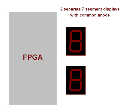
    FPGA dev boards usually have 4 or 6 seven segment displays. On some dev boards they are linked  to the FPGA to 7 pins for the data and one pin for the common element each like in the diagram:
    This type of connection is rare but if you have a board with 7 segment displays connected like this you will have a easier job using them in your projects.
    Another way these circuits are connected is with separate common elements (the same as in the picture above but with common data pins. These displays require a technique named multiplexing in order to use all the digits. This tutorial does not cover multiplexing so if you have a connection like this one all your digits will show the same number.
    
    You can tell from this picture that we can't use both the 7 segment displays in normal conditions because if we activate them both then the same character will be shown on them. If you have a dev board with the displays like this, you will see in a later tutorial how to send different data to every 7 segment cell.
   One last note: some boards have the common element inverted. Mine for example has a common anode display but the anodes are activated by a logic 0. The cathodes are normal (0-active). My board is a Digilent Nexys 3 so if you have it you're in luck. For other boards you have to figure it out for yourselves.

    From BCD code to 7 segment code
    BCD stands for binary coded decimal. A BCD code is a 4 bit number that ca represent the numbers 0-9 (0000, 0001, 0010, 0011, 0100, 0101, 0110, 0111, 1000, 1001). A BCD to 7 segment decoder maps each of these 10 codes to 7 bit codes (one bit for each segment) that will control the display.
    The chart for both common anode and cathode is:

    Decimal   BCD     Common anode     Common cathode
                                      gfedcba                 gfedcba

          0       0000          1000000               0111111
          1       0001          1111001               0000110
          2       0010          0100100               1011011
          3       0011          0110000               1001111
          4       0100          0011001               1100110
          5       0101          0010010               1101101
          6       0110          0000010               1111101
          7       0111          1111000               0000111
          8       1000          0000000               1111111
          9       1001          0010000               1101111

    Using this table you can make a decoder with the selected signal assignment or however you want. My example is for common anode but you can use the codes for common cathode and leave the rest of the program unchanged if you need them.
    Example for 0: I put the values from g to a so when we want to show a 0 only the g segment will be shut down (1 for common anode or 0 for common cathode).
    You can see that when we have an 8 all the segments are lit.

    The 7 segment decoder
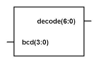
    The decoder will have 4 inputs of type std_logic or one input of type std_logic_vector(3 downto 0). I will be using std_logic_vector. The output is a std_logic_vector(6 downto 0). The decoding will be done with the selected signal assignment statement.
    The diagram :
    For implementation use 4 slide switches as inputs and the 7 data elements as outputs. The common element usually activates itself when not declared. If not then you must declare one more output of type std_logic and give it the value 0 or 1 depending on the element you have (anode or cathode).
    The code is:
    
    As you can see for other values other than 0-9 the LEDs will not light up. If you also need to declare the anode just put the declaration in the entity and then give it the value 0 or 1 in the architecture. 


Monday, November 28, 2011

Sequential statements

   In order to use sequential statements we need a special concurrent structure called a process because in an architecture body sequential code is not allowed so first let's see what a process is and how it fits in the description of a circuit.
    Here's a diagram of a VHDL program with processes:
    As you can see an entire process can be thought as a concurrent statement and the code inside it is sequential. This means that 2 processes execute concurrently relative to each other and other concurrent code but the statements inside them are sequential.
    A process has the following structure:
              name: process(sensitivity list)
                   variable declarations
              begin
                   sequential statements
              end process;

    The name: part is not mandatory but it helps you find a certain process when you have lots of them in the same vhdl file, although the same thing can be achieved by using comments. Variable declarations are also optional and we will get to them later in the tutorial.
    Let's see what the sensitivity list is. Basically a process executes only when it is triggered by an event (a signal that changes value) so we need to put all the signals that make the internals of that process in the list. Let's take for example a simple 3 input xor function (r<= a xor b xor c). The process for this code must have in it's sensitivity list all 3 input signals because we want the result r to be updated every time one of the inputs changes value. If for example in the list we would put only a then the result would be updated when a changes value but not when b or c change their values. This is a very important thing to remember for when you will design complex circuits. The process for this function looks like this:

              process(a,b,c)
              begin
                   r <= a xor b xor c;
             end process;
    
    Variables are used only in processes. A variable declared in a process is local to that process so you can have more processes with the same variables in a vhdl file. A variable can have all the data types a signal has and it is not that different from signals. Let's see how to declare and use a variable:

              variable count : integer;
              ...................................
              count := count +1;
              ...................................

    So the big difference between a signal and a variable is that a variable is assigned a value with  := .
    
    Sequential statements
    1)  Signal assignments:
         This is the same as in concurrent code but you have to be careful with the order in witch you put the statements because they execute one after the other.

              signal <= value;
   
    2)  Variable assignments:

              variable := value;

    3)  The if statement:
          This is a conditional statement in witch a block of sequential code is executed if a condition is true. The structure of the if statement is:

              if (expression 1) then
                  sequential block 1
              elsif (expression 2) then
                  sequential block 2
             ...............................
             else sequential block n
             end if;

          Another way to write an if statement is:

              if (expression 1) then
                  sequential block 1
              else
                  if (expression 2) then
                      sequential block 2
                  else sequential block 3
                  end if;
              end if;

          So in an if statement the first expression is evaluated and if it is true then the code attached to it is executed. If it is not true the next statement is evaluated and so on. 
          Let's see how the multiplexer from the last tutorials can be designed using the if statement:

              process (s,i0,i1,i2,i3)
              begin
                  if (s="00") then 
                      o <=  i0;
                  elsif (s="01") then
                      o <= i1;
                  elseif (s="10") then
                      o <= i2;
                 else o <= i3;
                 end if;
              end process;

          As you can see in the sensitivity list I have included s and the 4 inputs so that even if s doesn't change, the output will be updated with each input change. In order to test the code replace the concurrent statements from the other examples with the process. The entity is the same.

    4)  The case statement:
          This is similar to the with select statement. Let's see the structure:

              case expression is
                  when value 1 =>
                      sequential block 1
                   when value 2 =>
                       sequential block 2
                   ..............................
                   when value n =>
                       sequential block n
                   when others =>
                       other sequential block
              end case;

          The case is simple: a certain block of sequential code is executed based on the value of expression. Let's see the multiplexer with the case statement:

              process (s,i0,i1,i2,i3)
              begin
                  case s is
                      when "00" =>
                          o <= i0;
                      when "01" =>
                          o <= i1;
                      when "10" =>
                          o <= i2;
                      when others =>
                          o <= i3;
                  end case;
              end process;

    5)  The for loop:
          The for loop executes a sequential block of code over and over again for a number of times. It isn't used as much as the other 2 statements so that's why for now I won't be making an example for it. The structure of o for loop is:
             
              for index in range loop
                  sequential block
              end loop;

          We will use for loops in later tutorials.    


Monday, November 21, 2011

Designing a simple ALU with multiplexers

    What is an ALU? It is short for Arithmetic Logic Unit and it represents a circuit found in processors that performs different arithmetic and logic functions on 2 or maybe more operands. The basic functionality of an ALU is: it receives 2 operands on a number of bits and a select_operation signal that specifies the operation to perform and then outputs the result to another circuit like a register.
    The ALU we will design is very simple and you won't find such a circuit in any processor out there but it's a good circuit to see the application of multiplexers.
    Design data:
       - two 3 bit operands
       - a 3 bit result
       - a 2 bit select_operation input (so we will be able to have 2^2 operations)
       - 4 operations to perform (and, or, sum, xor)
   
    Note: the sum function is not a complete add operation because the operands and th result are 3 bits in length although the result should be of 4 bits ("111" + "001"= "1000"). Real adders will be covered in more advanced tutorials.

    The black box of the circuit:
    The entity should look like so:

    Another important thing to note is that in order to use the + operation you need the numeric library declared:
    use IEEE.numeric_std.ALL;

    Now let's talk about how the ALU will work:
    op1 and op2 are the 2 input operands. These will go through the 4 operations specified and the results will be put in 4 signals. Those signals represent the data inputs of the multiplexer and operation is the selection signal. The output of the mux is the result. So if we have op1="1010", op2="0010" and operation="10" witch will be addition then the result will be result="1100".
    
    Let's see the internals of the ALU:

    This is the basic structure of an ALU. The circuit can be described using data flow or structural description. Because the operations we are using are simple it's better to use data flow but when designing advanced ALUs with complex operations it's better to describe it using structural description.

    The code is:

    Perhaps an explanation is needed for sum:
    unsigned(op1) and unsigned(op2) transforms the std_logic_vector type into unsigned type in order to do the + operation (that's why we imported the numeric library). After the operation is done we need it in std_logic_vector form so we use std_logic_vector(unsigned(op1)+unsigned(op2)). It is like using a signal addition of unsigned type to store the addition result and then converting it like so:
       signal addition:unsigned(2 downto 0);
       
      addition<=unsigned(op1)+unsigned(op2);
      sumsig<=std_logic_vector(addition);

    This is just one of the applications of multiplexers. As the tutorials get more complex you will see more and more situations in witch you will need these circuits.


Saturday, November 19, 2011

Concurrent statements

    Until now you have seen how to transform a truth table in concurrent signal assignments or in processes. But not every circuit can or should be described only with logic functions. That's why VHDL has 2 concurrent signal assignment statements:
       - conditional signal assignment
       - selected signal assignment

    In order to demonstrate these 2 statements we will design 2 circuits: a 4 to 1 multiplexer and a 2 to 4 decoder. Let's see first what these circuits do:
 
    4 to 1 multiplexer
    Such a circuit has 4 data inputs, 2 select inputs and 1 output:

    This is the basic I/O of any mux. The 4 inputs can be of any bit length (from 1 bit to what your design needs). The s input can also be of different bit lengths but one rule needs to be respected: number of inputs=2 to the power of s. So if you want a 2 to 1 mux you will need a 1 bit select signal. For a 4 to 1 mux the s signal needs to be 2 bits in length. The output o will receive one of the inputs based on the value of s.

       s    o
      00   i0
      01   i1
      10   i2
      11   i3
    This is the table that a multiplexer follows.

    2 to 4 decoder
    A n to 2^n decoder takes n inputs that act similarly to the s input of the mux and outputs a 2^n value based on the input value. Let's see how a decoder looks:
    The table for a decoder is:
       
       i       o
     00    0001
     01    0010
     10    0100
     11    1000
   
    The circuits works exactly as you see in this table so no further explanations are needed.

    Entity coding
    The entities for the 2 circuits should be like:
    For the mux and for the decoder:

    Conditional signal assignment
    This type of statement is not the best way to describe the 2 circuits because it is priority based but it is a good way to understand how to use it.
    The structure of the statement is:

    output <= input1 when condition1 else
                    input2 when condition2 else
                    ..........................................
                   inputn;

    As you can see the program will evaluate the first condition and if it is true the output will get the input1 value. If condition1 is false then condition2 will be evaluated and so on. If none of the conditions are true then output will get the inputn value.
    This is the reason I recommend not to use this statement to describe multiplexers and decoders/encoders. The conditional signal assignment is best suited for priority encoders and other such circuits.

    The VHDL code for the 4 to 1 4 bit multiplexer:

    The VHDL code for the 2 to 4 decoder is:

    Selected signal assignment
    This type of assignment is the best way to describe multiplexers and decoders because they are not priority based.
    The structure of the statement is:
    
    with select_signal select
           output <= value1 when select_sig_value1,
                           value2 when select_sig_value2,
                           ..............................................
                          valuen when others;

    So the output will get one of the n-1 values depending on the select_sig value. If none of the values specified are met then the output will get valuen.

    Let's the code for the mux and the decoder:


    Implementation
    For implementation the outputs will be set as LEDs for both the multiplexer and the decoder. The s and i inputs will be slide switches.
    For inputs i0-i3 you can assign constant values in code and see how they are routed to the LEDs with the values from the switches.
   

Friday, November 11, 2011

VHDL design types

    As you have seen a VHDL described circuit has 2 main parts: the entity and the architecture witch contains the functionality of the circuit. There are 3 ways to describe digital circuits in VHDL:
       - Dataflow
       - Behavioral
       - Structural

    In this tutorial I will describe the same circuit using all 3 types of description so you can see the difference between them.
 
    The designed circuit
    A very simple but useful circuit is the parity detector. To determine the parity of a binery number we need to count the '1' bits. If that number is even than it is of even parity. If it's odd than the number is of odd parity. My tutorials will describe a circuit that outputs the even parity.

    Parity detector with 3 inputs and 1 output truth table:

       A  B  C   O
       0   0   0    1
       0   0   1    0
       0   1   0    0
       0   1   1    1
       1   0   0    0
       1   0   1    1
       1   1   0    1
       1   1   1    0
    So when the number of '1's is enev the output is '1' and vice versa.
    As you can see the truth table is rather large so it needs to be minimized. Since logic function minimization is out of the scope of this tutorial I will not be presenting it but there are lots of articles on the internet about the ways to do it.
    The circuit we will describe looks like this:

    There are other ways to design the logic diagram but using XOR gates is the most simple circuit for detecting parity.
    Regardless of the way we will describe the circuit, the entity will remain the same:
    

    Dataflow description
    In dataflow we describe circuits using only concurrent statements, mainly signal assignments. 
    A signal can be seen as a wire between 2 circuits. For example in the upper diagram abSIG is a signal that connects the first XOR output with the second XOR input.A, B, C and O are signals also but they connect the entity with the FPGA pins. 
    For this circuit we can use a description with signals or we can write the whole logic function in one statement. I will demonstrate both approaches.
    
    Without signals:
    You just have to write in the architecture 
              o <= not(a xor b xor c);


    With signals:
    For this method we need to declare 2 signals like those in the diagram. They will be of type STD_LOGIC. 
    The code looks like this:


    Remember that the order of the statements is not set in stone because they take effect at the same time. 

    Behavioral description
    This type of description uses sequential code that needs to be written inside a structure named process. The process is located in the architecture body and there can be more of them in the same architecture. Processes execute concurrently with each other but in each process the code is sequential.
    Declaration of a process:
              name: process(sensitivity list)
    The name is not necessary but when you have lots of processes it helps to easily find the one you want. The reserved word process is mandatory.
    The sensitivity list is a list of signals that control the entrance in the process. That means that when a signal in the list changes value the process will execute it's code so you need to be careful to put all the necesary signals in that list.
    After this line we can declare variables to use for the process. Variables, if you recall are local to each process they are declared in and help you build complex algorithms and circuits.
    The code of the process comes next. It is enclosed in begin-end statements.
    For this example we will not be using variables. The code looks like:

    If you look at the sensitivity list you can see that every time one of the inputs changes it's value the process will run o will take a new value.
    If we use signals the code will look exactly like for dataflow but it is important to keep it exactly the same because in processes code is sequential. This means that if you decide to put the o assignment first your code will be incorrect.

    Structural description
    This type of description is mostly used for more complex projects because you can segment your code in smaller circuits and connect them together using signals, hence the word "structural". 
    For our circuit we will need to make a description for the xor gate and one for the not gate. After that we will make another description of the main circuit in witch the others are connected.
    Because this method is more complicated I will be walking you through the steps.
    First create a new project with and give it a name:

    After that set your device parameters, click next and click finish.
    We are ready to start the coding. Create an entity and name it xorGate. It will have 2 inputs (i0 and i1) and 1 output (o). After it is created write in the architecture body: o <= i0 xor i1;

    Now create another entity named inverter. It will have 1 input (i) and 1 output (o).

    These are the 2 circuits needed for the main architecture.
    Before we continue let's see a block diagram of our project:

    As you can see the main description will have 3 inputs (A, B and C) and 1 output (O). 
    Because The main circuit and the 2 gates are in different files we need a way to link them. This is done of course in the main file using components. They are declared before the architecture begins (with the signals). There will be a component for each type of circuit (in our case one for andGate and one for inverter) and the structure of the component is exactly like that of the entity with 2 differences:
       - instead of the entity keyword at the beginning we will use component
       - instead of the name of the entity at the end statement we will use component as well

    Let's create a new entity called parityDetector with the I/O specified and declare our 2 components:

    After the components we need to declare our signals. These are used to link the components together.

    Now it's time to link the components. Because there are 3 circuits in the block diagram we will be instantiating 3 components (2 xor gates and 1 inverter). 
    Each instantiation has 3 parts:
       - A label that has to be unique for each component instantiation. It is placed first and it should have a suggestive name for that circuit
       - The name of the component instantiated (the same name of the entity for the specific circuit)
       - The reserved words "port map" followed by a list of signals in parentheses. The signals are the ones specified in the main entity (either the I/O of that entity or declared signals) and need to be placed in the order that the component has it's I/O placed. For example the inverter has it's I/O signals in the order: i,o so the instantiation for it would be:
              INV: inverter port map(parity, O);
    From that piece of code we conclude that the signal parity witch is also linked to the output of an xorGate is linked to the i pin of the inverter and the main output of our circuit: O is linked to the output pin of the inverter (o).
    The code looks like this:

    So the XORG1 circuit will compute an xor operation on A and B and communicate the result to XORG2 through the abSIG signal. XOR2 calculates abSIG xor C and gives the result to the inverter using the parity signal. The inverter performs the not operation and sends the result to the main output of the circuit. The order is not important because they are concurrent statements.
    So the structural design is similar to a schematic design because we connect circuits with wires (signals). It is best used in more complex projects.
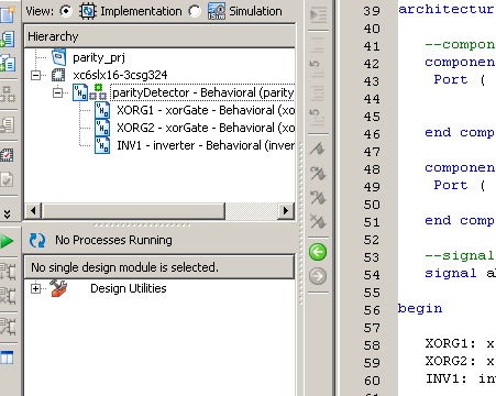
    After you do the last bit of code save the project and the parityDetector entity should become the top level module:

    Next put in the user constraints, implement and see the results. 
    For all the examples in this tutorial the inputs should be 3 slide switches and the output a LED.